Toray Industries advances microfabrication with high-aspect-ratio polyimide STF-1000, enabling durable thick-film patterning for MEMS, semiconductors, and next-generation electronics.
Japanese chemical giant Toray Industries is preparing to begin large-scale production of its advanced STF-1000 photosensitive polyimide, an innovative material poised to transform microfabrication technologies. The company describes this development as the outcome of its continuous efforts to advance its proprietary negative-type photosensitive technology, pushing the boundaries of what is possible in high-performance materials.
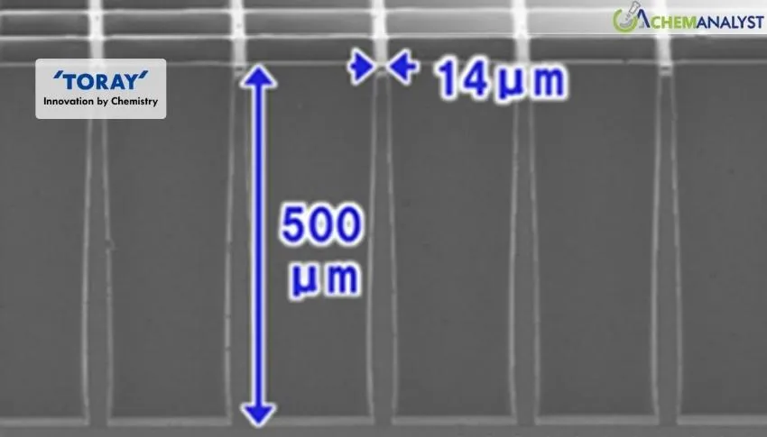
The STF-1000 material introduces a remarkable breakthrough by enabling pattern formation with an exceptionally high aspect ratio of 36, even in films as thick as 500 micrometers. High-aspect-ratio structures, which are both tall and narrow, are essential for next-generation electronic devices and micro-electromechanical systems (MEMS). These structures play a critical role in improving performance, miniaturization, and efficiency in advanced technological applications.
Toray had already initiated sample shipments of STF-1000 in the previous year, allowing customers across industries such as electronics and MEMS to evaluate its capabilities. MEMS technology, which integrates tiny mechanical components, sensors, and actuators using semiconductor fabrication techniques, is rapidly expanding due to increasing demand for compact and multifunctional devices.
The innovation behind STF-1000 has also received industry recognition. It was honored with the The Chemical Society of Japan Award for Young Chemists in Technical Development, underscoring Toray’s success in maintaining the core benefits of polyimide materials while achieving superior patterning performance. These inherent properties include excellent thermal stability, chemical resistance, mechanical strength, electrical insulation, and resistance to ultraviolet radiation.
The material relies on photolithography, a crucial process in modern electronics manufacturing. Photolithography involves coating a substrate with a photosensitive material and then exposing it to light to create highly precise patterns. This method is fundamental to producing semiconductors, liquid crystal displays, and various types of sensors.
As electronic components continue to shrink in size while increasing in functionality, the demand for materials capable of supporting dense integration has grown significantly. Toray highlighted that conventional materials often struggle when film thickness exceeds 200 micrometers, leading to issues such as cracking or delamination. STF-1000 overcomes these limitations through an enhanced polymer design tailored for negative-tone photosensitive materials. This innovation minimizes pattern distortion and prevents structural damage, even in thicker films.
Beyond its core applications, STF-1000 is versatile enough to support a wide range of pattern designs, including semiconductor vias and MEMS structures. It is also suitable for use in scintillator panels employed in X-ray non-destructive testing systems. Looking ahead, potential applications extend to advanced semiconductor devices and emerging microfluidic technologies.
In addition to STF-1000, Toray introduced STF-2000 in 2025, a new photosensitive polyimide formulation that eliminates per- and polyfluoroalkyl substances (PFAS). This development aligns with growing environmental concerns while maintaining strong performance for electronic and microfluidic applications.
Moving forward, Toray plans to build on its expertise in organic synthesis, polymer science, biotechnology, and nanotechnology to further strengthen its research and development capabilities. The company remains committed to creating innovative materials that not only enhance technological progress but also contribute positively to society.